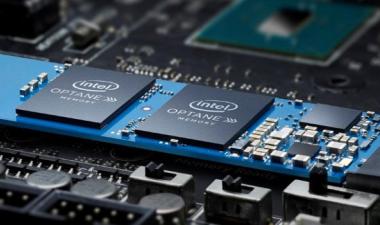
Intel's 2n一代xpoint记忆 - 值得一直很长的等待吗?
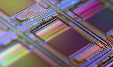
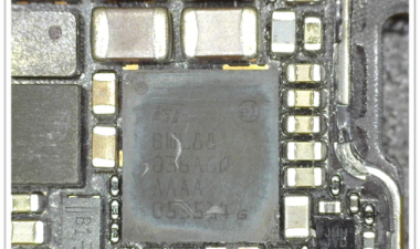
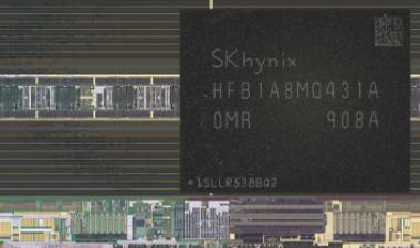
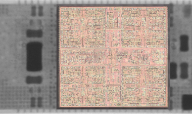
2017年,TechInsights分析了英特尔1的细节英石根本。XPoint Memory (OptaneTM内存16GB,MEMPEK1W016GA)包括结构,材料,工艺,设计和电路。从那时起,我们一直在等待2n根本。XPoint Memory for many years. 3D XPoint non-volatile memory technology was introduced in 2015, and products started shipping from 2017. Micron’s strategy was providing data center customers such as Intel with persistent memory technology for cloud-native infrastructure. The initial value proposition was higher density, cheaper DRAM, and faster NAND. However, Micron decided to exit 3D XPoint non-volatile memory market, instead focusing its data center efforts on the emerging Compute Express Link (CXL) interface. As Micron Technology just gave it up recently although they have 1英石XPoint Memory products (X100 SSDs) for limited customers, Intel is now the only company on this.
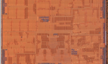
Intel has announced three new memory products in the Optane family with 2n根本。3D XPoint Memory last December. The 2n根本。XPoint存储器具有四层相变存储器(PCM)结构,用于256GB模具。据说Optane P5800X是市场上最快的企业SSD,在市场上有PCIe NVME 4.0 x4。
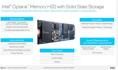
There is also a new hybrid SSD with NAND and 3DXP as well as a new generation of Optane DIMM with Crow Pass. The Optane Memory H20, an SSD that combines a large part of 3D NAND with a small part of 3D XPoint, appears under the code name Pyramid Glacier. The introduction of the Intel Optane H20 SSD is scheduled for the second quarter of 2021. The third generation of the Optane Persistent Memory, also known as Optane DIMM, is now on the agenda with Crow Pass, which is only due to appear with the upcoming Sapphire Rapids server platform, which is not expected until the end of 2021 at the earliest.
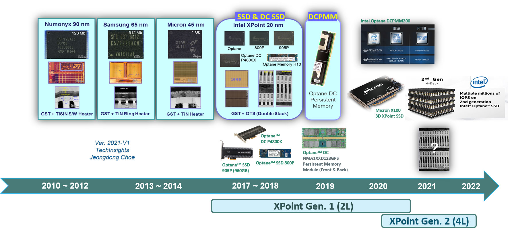
Figure 1. History of XPoint and PCM devices revealed on the market
In the meantime, we’d better briefly recall and review the 1英石根本。XPoint存储器技术,尤其是结构,材料和模具/块设计。图1显示了XPoint / PCM历史记录。第一个。XPoint存储器管芯具有128GB(16GB)管芯密度和两层PCM结构。它已被使用许多Intel SSD产品,如OpteN,800P,900P,DC P4800x,H10和DCPMM。
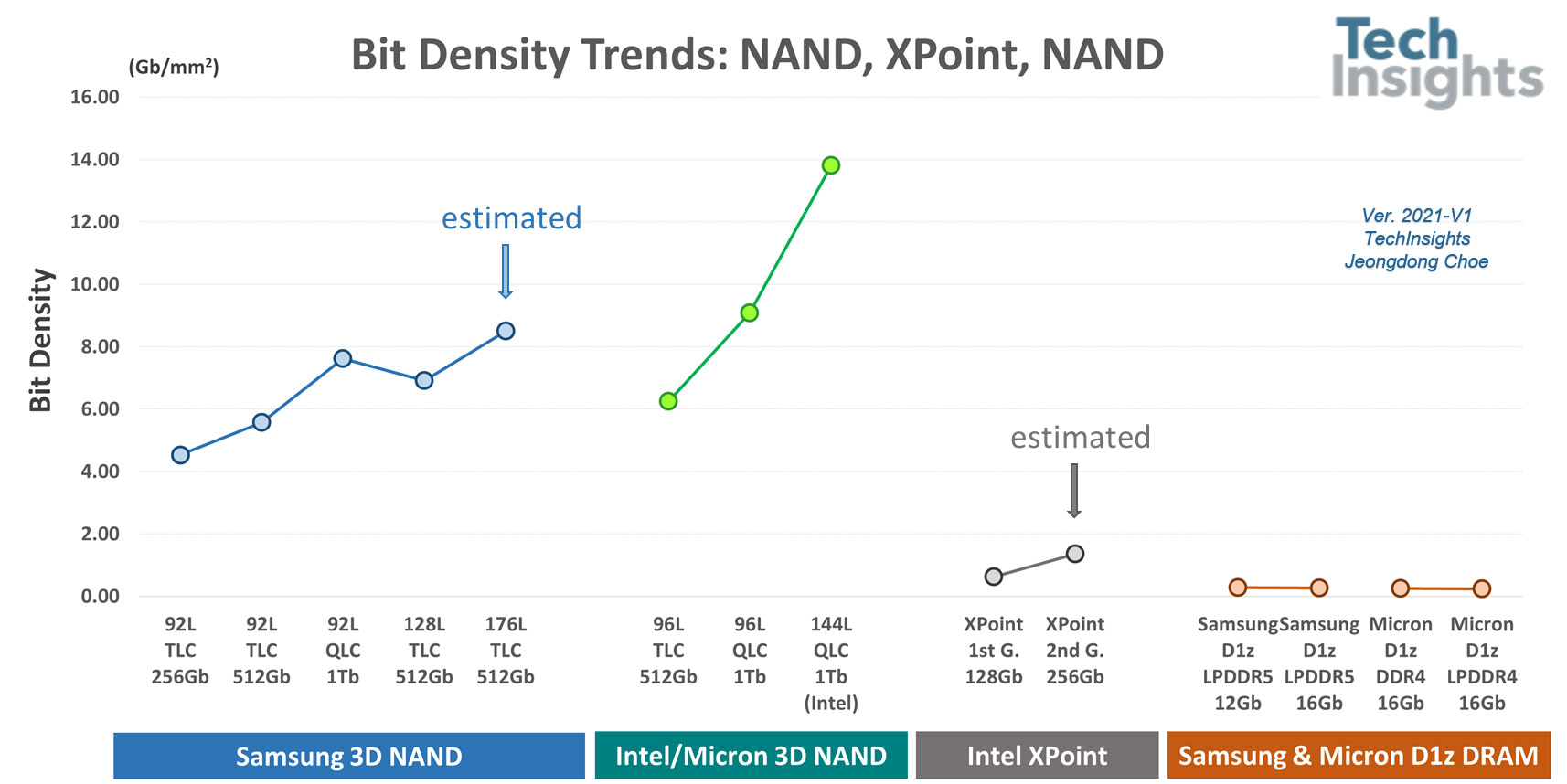
图2。位密度的比较;3 d NAND摇来摇去m Samsung, Intel and Micron, Intel XPoint, D1z DRAM from Samsung and Micron
When it comes to memory bit density, Intel Optane XPoint 1st gen. has 0.62 Gb/mm2,高于DRAM模具(平均比特密度0.23〜0.27 GB / mm2for D1z node DRAM products), while quite lower than currently commercialized 128L or 144L 3D NAND products, for example, Samsung 128L 512Gb TLC (6.91 Gb/mm2),SK Hynix 128L 512GB TLC(8.11 GB / mm2) and Intel 144L QLC (12.86 Gb/mm2)。图2显示了比特密度的比较;3D来自三星,英特尔和微米,英特尔Xpoint,来自三星和微米的D1Z DRAM的NAND。我们估计并添加了上行的三星176L 512GB TLC 3D NAND和英特尔第二型。XPoint存储器256GB进入图形。如果是第二局。XPoint Memory 256GB管芯具有相同的芯片尺寸和良好优化外设设计,它增加到约1.36 GB / mm2,但是仍处于N1Y或N1Z 2D Nand的范围内。对于更高密度存储类存储器(SCM)应用,将需要更具创新性和新的架构概念。
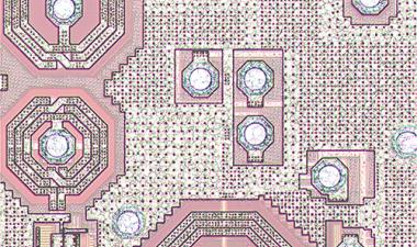
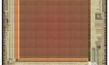
英特尔XPoint单元阵列结构和外设设计使用CMOS的概念在阵列(CUA)下,其也用于英特尔/微米3D NAND建筑。通过CUA型集成,英特尔和微米的3D NAND内存阵列效率比非CUA产品(60〜70%)更高(〜85%)。同样地,XPoint存储器管芯的存储器效率大于90%,因为XPoint存储器阵列中的存储元件位于金属4和金属5之间。换句话说,所有CMOS电路,如驱动程序,解码器,BL访问,本地数据等地址控制放置在内存元素下,类似于3D NAND的CUA架构。外围模具设计,设计与瓷砖型铺板平板,与英特尔/微米CUA 3D NAND模具相同。每芯片的16,384块瓷砖是指7.81 MB /瓷砖密度,并且每块瓷砖2,150BLS和2,150 WLS,包括伪WLS和BLS。
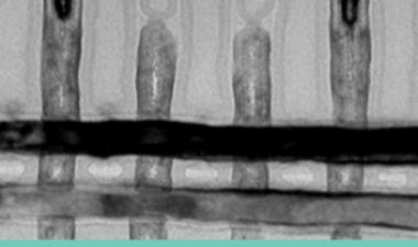
A double layered storage/selector structure was used for the 1英石根本。xpoint内存。对于存储元件,已经提出并开发了许多候选者,例如相变材料,电阻氧化物电池,导电桥电池和MRAM电池。其中,1英石根本。XPoint内存采用基于硫属化物的相变材料,GST(GE-SB-TE)合金层。用于BL和WL光刻/蚀刻工艺的20nm双图案化技术(DPT)。有效地,设计在XPoint存储器单元阵列上的2F2单元。
For the selector elements, many of switching devices such as a transistor-type (BJT or FET), diode-type and ovonic threshold switch can be used. Intel 1英石根本。XPoint Memory uses another chalcogenide-based alloy with arsenic (As) doped, which is different from GST alloy PCM layer. The selector material Intel used is an ovonic threshold switch (OTS) material. The overall structure consists of a double stacked memory layers and OTS selector elements along bitline and wordline. OTS selectors are not extended over middle electrode or bottom electrode.
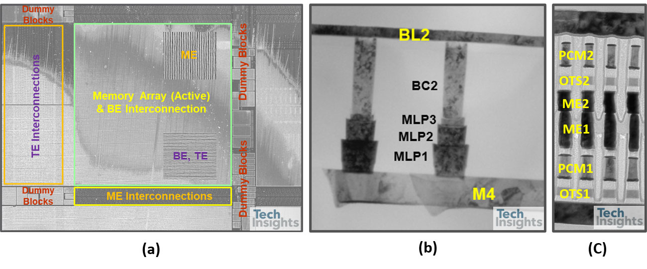
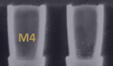
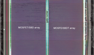
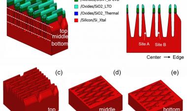
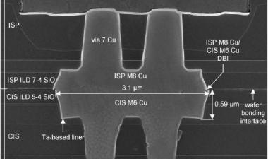
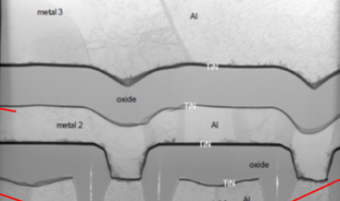
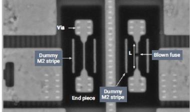
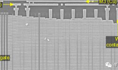
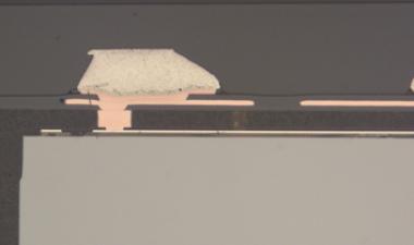
图3:描述过程和设计的一些问题的图像;(a)在活性阵列附近的凹陷块和互连区域,(b)M4上的多垫,(c)PCM / OST细胞结构,ME1钨层分开2
Some of issues to be improved on process and design were there, for example, array and peripheral area mismatch, throughput/cost, WL/BL interconnection area penalty, and cell scaling. Figure 4 shows some images describing the issues including (a) dummy blocks and interconnection area near active array, (b) multi-pads on M4, and (c) PCM/OST cell structure with ME2 tungsten process separated from ME1. Peripheral area is not well matched to the XPoint cell array area, which causes a lot of dummy cell blocks added between the active cell blocks. Due to the area penalty, cell area efficiency decreased to 57.8% although they use CuA structure. Three landing pads are used under WL, BL1 and BL2 contacts to connect with M4 layer on cell XPoint array, which may cause higher Rc and increase cost. Middle electrode (ME) layer consists of two separated W layers, ME1 and ME2, which means additional photolithography, etching and CMP processes are needed.
Why are we patiently waiting for the 2n根本。xpoint内存?
We expect many of the issues would be solved and improved from Intel for the 2n根本。XPoint Memory products. We’re looking forward to finding how Intel update the XPoint technology.
Dr. Jeongdong Choe那Senior Technical Fellow
Dr. Jeongdong Choe is a Senior Technical Fellow at TechInsights. He has nearly 30 years of experience in the semiconductor industry, R&D and reverse engineering on DRAM, NAND/NOR FLASH, SRAM/Logic and emerging memory. He worked for SK Hynix and Samsung Electronics for over 20 years. He joined TechInsights and has been focusing on technology analysis on semiconductor process, device and architecture. He has written many articles on memory technology including DRAM technology trend, 2D and 3D NAND process/device integration details, and Emerging memory such as STT-MRAM, XPoint, ReRAM and FeRAM design and architecture. He quarterly produces and updates a widely distributed memory roadmaps on DRAM, NAND and Emerging memory.
想阅读更多?
TechInsights.记忆订阅rs already have access to exclusive content in the TechInsights Platform.