Posted: April 24, 2017
撰稿人:Andy Wei
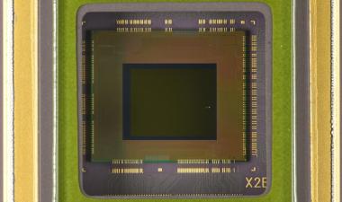
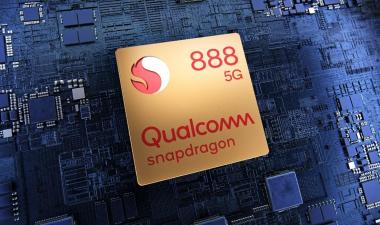
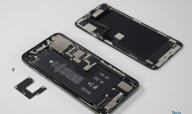
用第一套三星Galaxy S8拆除那we have access now to the first SoCs produced on “10 nm” class technology. First to the 10 nm productization finish line is the Qualcomm Snapdragon 835, built on Samsung LSI Foundry’s 10 nm LPE technology. In parallel, Samsung’s own Exynos 8895 was released concurrently, and we expect to find these in our second set of Samsung Galaxy S8 teardowns.
The Qualcomm Snapdragon 835 has a die size of 72.3 mm2。Compared to the die size of the Snapdragon 820 at 113.7 mm2那this represents a 36% die size shrink. The Qualcomm Snapdragon 835 appears to be mainly a shrink of the Snapdragon 820/821 family, with upgrades in similar IP blocks, but no new major IP blocks have been added. There is, however, a major change in the CPUs. The Snapdragon 820 family used a very large area 2+2 big-little implementation which seemed out of place in a mobile applications processor. We suspect the Kyro was a re-use of cores designed for Qualcomm’s ARM server ambitions. The Snapdragon 835 uses a more ARM-like 4+4 big-little implementation in the Kyro 280, which are a derivative of the ARM Coretex-A73/A53 implementation we have already seen in the HiSilicon Kirin 960.
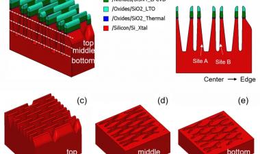
Complimentary Floor Plan (Annotated Die Images) & Product Brief - Samsung 10 nm Process
Qualcomm Snapdragon 820/821在三星14 LPP vs Snapdragon 835上Samsung 10 LPE

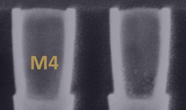
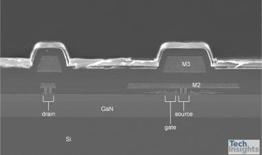
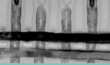
10nm的扫描电镜截面
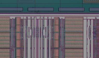
CPU的这种重大变化偏离整体芯片尺寸减小,具有更明显的规模因素的外观。但是,在具有更多微小变化的功能块中查看功能块,例如adreno 530到adreno 540 gpu mp单元,我们看到更接近25%的面积尺度。无论这是否指示真正的比例因子,或者这是复杂性的并发增加的结果,以利用面积尺度,不可能确定而无需进一步分析。为了评估Qualcomm对三星的10 nm LPE技术的实施,我们必须在功能块水平和标准单元格层面上详细介绍,以规格栅极密度增益和每个门缩放改进的成本。为了准确评估,我们在功能块水平,标准电池和利用率,过程分析和晶体管表征中发起了广泛的分析。我们可以将这些与Samsung 14LPE和14LPP的分析进行比较,以获得实际规模因子,成本规模和性能差异。然后,我们将其与我们在英特尔,Apple,Mediatek,Hisilicon等的分析图书馆进行比较。
这是一个激动人心的时刻。在克服物理扩展限制并保持传统成本和性能扩展的高度创新中,我们正在分析“10nm”级技术的首次进入。与14/16海里的所有选手相比,这一成绩如何?尤其是,英特尔最近向业界提出了一项挑战,即将实际晶体管密度作为一项技术指标来报告,这与此有何关系?随着我们的分析开始深入到门的层次,更多的细节将会出现。