Posted: June 05, 2020
Contributed by: Sinjin Dixon-Warren, PhD
电力电子行业处于过渡时期。多年来,基于硅的设备占主导地位,传统的SI MOSFET晶体管用于较低的功率和中频,具有超级接合(SJ)MOSFET器件用于更高的频率和更高的电压,并且用于高频率和更高的电压,并且IGBT器件用于高频率和更高的电压电源和较低频率。传统的SI MOSFET和SJ MOSFET通常在消费者应用中发现,例如移动交流适配器,而IGBT用于工业,混合动力和电动车辆(EV)应用,太阳能应用以及大型电源。
氮化镓(GaN)和碳化硅(SIC)是在过去十年内出现在市场上的较新的,宽的带隙(WBG)技术,其目的是取代这些硅技术。碳化硅显示有望取代IGBT技术,因为它能够以更高的频率和更高的损耗在更高的温度和更高的功率下操作。氮化镓主要是置换SJ MOSFET技术,也是由于其在较高频率下运行的能力,较低的损耗。GaN,SIC和SJ MOSFET技术直接竞争650 V套接字胜利,目前尚不清楚哪种技术最终将在这种中间电压电压级别占据市场。
基于GaN-on-Si的高电子迁移率晶体管(HEMT)是GaN电力电子领域最有前途的新兴技术。它们是一年一度的电力系统与设备国际研讨会(ISPSD)和应用电力电子会议(APEC)的常规议题。
HEMT装置的发明通常归因于Takashi Mimura,1979年在日本富士通工作的物理学家。HEMT设备的原始基础是GaAs。在GaAs衬底的表面上形成薄层AlgaAs,导致在AlGaAS / GaAs接口处形成二维电子气体(2deg)层。调制2DEG的电导率构成了HEMT器件的基础。Takashi Mimura于1979年提出了本发明的专利,JPS5953714B2(另见CA1145482A)
这physical properties of gallium nitride mean that GaN HEMTS, which are based on an AlGaN/GaN interface, should feature low on-state resistance, due to the high mobility, and low switching losses, due to the wide bandgap, as compared to Si power transistors. The technology has application for power switching transistors in voltage converter applications. Unfortunately, GaN materials properties have made the commercialization of GaN devices challenging. It is only in the past decade that commercial GaN HEMT power electronics technology has appeared on the open market.
GaN HEMTs were first patented in 1991 underUS5192987A('987专利)由M.A. Khan,J.M.Vanhove,J.N.Kuznia和D.T. Olson在APA Optics Inc.在明尼阿波利斯,MN。它是一种装置(或机器)专利。该专利是题为“具有GaN / Alx Ga1-X N异质结的高电子迁移率晶体管”,并且摘要总结了如下:
公开了一种高电子迁移率晶体管,其利用由于在GaN / Alx Ga1-x N异质结中发生的二维电子气体而增加的迁移率。这些结构使用低压金属化学气相沉积在基底平面蓝宝石上沉积。异质结的电子迁移率在室温下为约620cm 2,与180℃下的56cm 2相比,每个伏特第二,并在77°K下减少到每伏第二厘米2cm 2。然而,对于异质结构的迁移率,在77°K时增加到每伏的每伏的1,600cm 2的值,并在4°K下饱和。
APA Optics还申请了第二种方法(或过程)专利,US5296395A,描述了GaN HEMT装置的制造。APA光学仍在继续存在。2004年,公司名称已更改为APA企业,并于2008年被重新标记为Clearfield Inc.该公司现在在墨西哥蒂华纳省蒂华纳的第二厂中提供了默认公司的纤维光学元件。然后将两项专利重新分配给国际整流器,现在是英飞凌的一部分。这两个精灵甘专利现在已经过期,因此呈现的概念是免费的。
在这篇简短的文章中,我们计划回顾GaN-HEMT的发明,如APA光学的987装置专利中所描述的,然后将其与目前商业化的GaN-HEMT技术进行比较。这一信息最初是为在亚太经合组织2020年会议上发表和一次会议准备的TechInsights.网络研讨会。
这Claim 1 of the ‘987 APA Optics GaN patent describes the essential concepts of the invention, which are generally applicable to current commercially available GaN HEMT power devices. We have underlined the key claim elements of the patent.
一种晶体管,包括:
- 底物;
- a buffer, the buffer being deposited on the substrate;
- 第一主动层,第一有源层基本上由GaN组成,第一有源层被沉积在缓冲液上;
- a second active layer, the second active layer being composed essentially of Alx Ga1-x N, where x is greater than 0 and less than 1; and
- a plurality of electrical connections, the electrical connections residing on the second active layer, the plurality of electrical connections comprising:
- 源连接,驻留在第二个活动区域上的源连接;
- a gate connection,位于第二有源区上的栅极连接;
- 排水连接, the drain connection residing on the second active region;
图1示出了来自'987 APA光学GaN HEMT专利的图像,其示出了本发明的基本概念。上面带下划线的密钥索赔元素被映射到图中的图表上。本发明包括形成在基材上的GaN的异质结构。在GaN第一有源层和薄的AlGaN第二有源层之间的界面处形成2deg形式。在AlGaN第二有源层上形成源极,漏极和栅极连接,从而形成HEMT装置结构。通常,晶体管将表现为常开(耗尽模式)设备,当栅极没有偏置时是开启的。
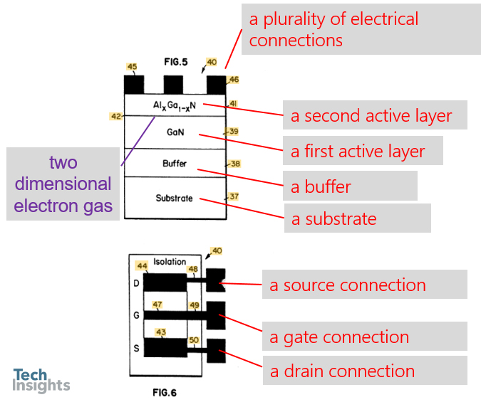
图1 US5192987A图6
通过逆向工程和专乐动篮球快讯利分析,我们已经能够在多个最新的GaN电力电子产品中观察到APA光学专利987的关键权利要求要素,例如,来自国际整流器、GaN系统、纳维、英飞凌、松下、高效功率转换、ONSemiconductor、,Transphorm和Texas Instruments。我们将在这里回顾两个选定的示例。在我们的文章中给出了进一步的例子APEC 2020.演示文稿和TechInsights网络研讨会。
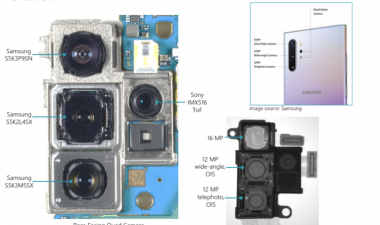
International Rectifier was first to market with a GaN-on-Si power device, the IP2010PBF GaN-Based Power Stage, which was released in February 2010. International Rectifier was an American semiconductor company, founded in 1954. In 2015 it became part of Infineon. As shown in Figure 2, the IP2010PBF comprises a GaN-on-Si HEMT, co-packaged with an ASIC. The GaN-on-Si die features two separate power transistor blocks, that are wired in a high side/low side bridge configuration.
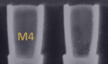
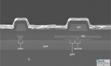
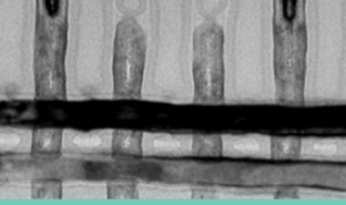
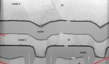
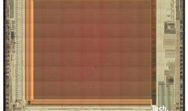
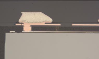
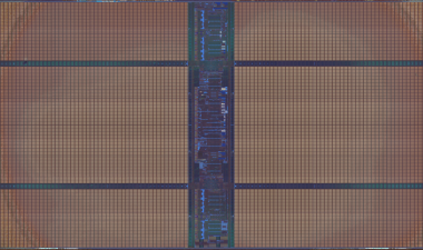
图3显示了IP2010PBF GaN-On-Si HEMT模具的一般结构的横截面TEM显微照片。“987专利”的关键索赔元素已映射到此图像上。在该模具上也执行电测量,确认它作为晶体管操作,如“987专利”所要求的。
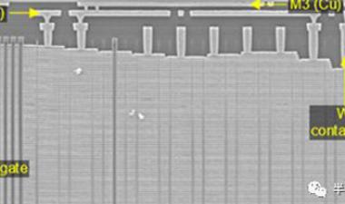
More detailed cross-sectional TEM micrographs of the contact and gate regions are presented in Figure 4. An ohmic metal 0 contact layer is used to make the source/drain electrical connection to the 2DEG that lies at the interface between the AlGaN second active layer and GaN first active layer. The device will feature normally-on operation, due to the presence of silicon nitride gate dielectric between the TiN gate material and the AlGaN. The presence of a gate dielectric is not explicitly described in the ‘987 patent, rather the patent describes the use of Schottky gate contacts. Schottky gates are not typically used for power electronics applications, but they are normally used for high frequency RF GaN HEMT devices.
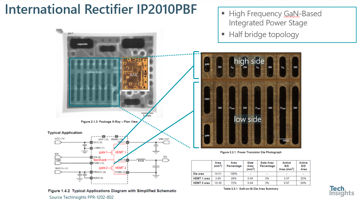
图2国际整流器IP2010PBF GAN的功率级
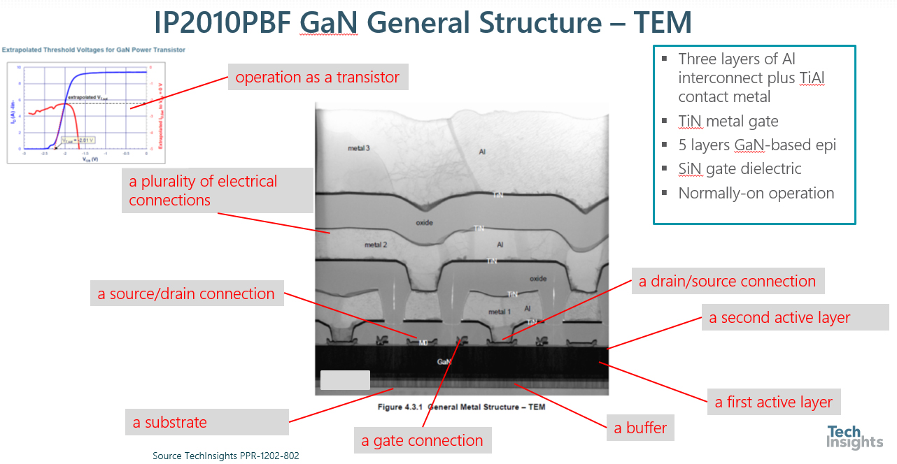
图3国际整流器IP2010PBF通用设备结构 - TEM
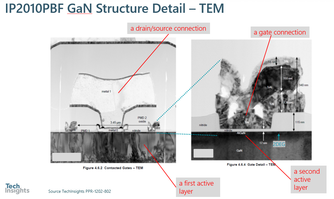
Figure 4 International Rectifier IP2010PBF General Device Structure – TEM Detail
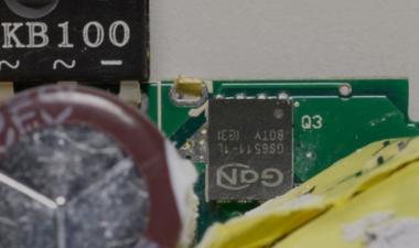
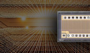
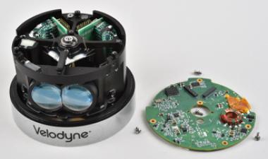
Navitas Semiconductor是一家美国单片集成(GanFastTM)GaN-On-Si功率IC的美国制造商。它们位于加利福尼亚州的El Segundo。在2018年在APEC上,Navitas宣布NV6252 650 V集成GaN半桥,专为主动钳位反激应用而设计。TechInsights最近发现了Aukey PA-U50 USB墙上充电器中的NV6252设备。
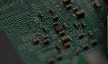
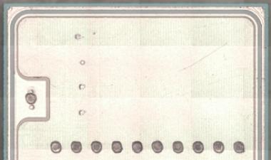
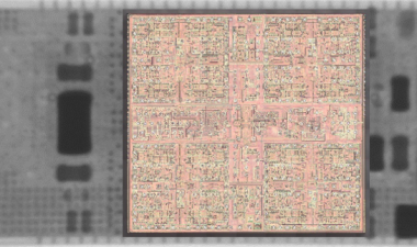
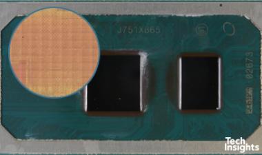
图5示出了从Aukey PA-U50提取的主PCB的照片。还示出了图5中的图5是NV6252器件的平面图X射线图像。在X射线中可以看到两个模具,其中模具标记NV6H002和HV6L002分别对应于半桥的高侧和低侧晶体管,在X射线中看到。从设备的设备框图datasheet,显示在X射线图像下方。
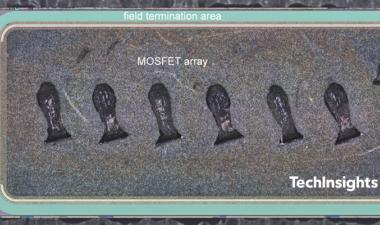
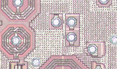
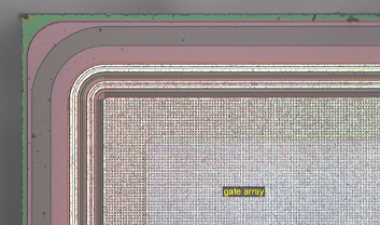
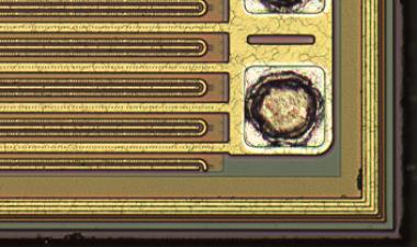
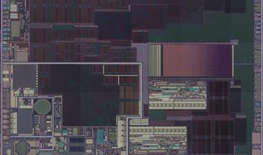
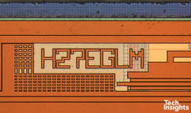
图6中所示的HV6H002高侧模具的一张照片伪造到晶体管栅极电平。在模具的右下角观察到功率晶体管块,而一块模拟电路围绕顶部和左侧死亡。根据“987专利”,大功率晶体管的存在确认该装置作为晶体管操作。
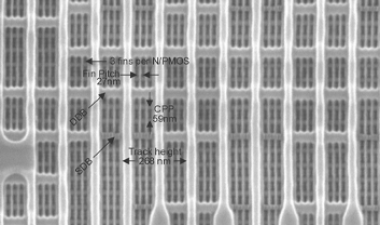
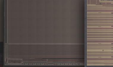
Figure 7 shows plan-view and cross-sectional SEM micrographs of transistors in the analog regions of the HV6L002 low side die found inside the NV6252. The key claim elements of the ‘987 patent have been mapped onto these images. Examination of the gate region of the transistors shows the presence of a mesa structure beneath the gate contact. This mesa is formed of P-type GaN and it forms the actual gate of the transistor. The presence of the P-type GaN in this mesa results in the depletion of the carriers in the 2DEG, thus giving rise to normally off (enhancement mode) operation. This concept was not anticipated in the original APA Optics patents, but is preferred in power electronics applications.
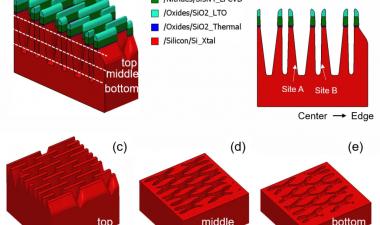
最后,图8显示了GaN基础外延的横截面SEM和TEM显微照片,用于形成NV6252模具。使用10层GaN的外延,包括两个超级晶格结构。尽管额外的复杂性,但是继续支持'987专利的关键要素。
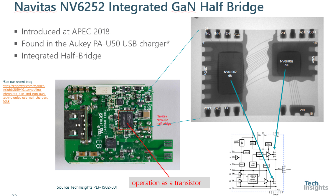
图5 Navitas NV6252集成GAN半桥
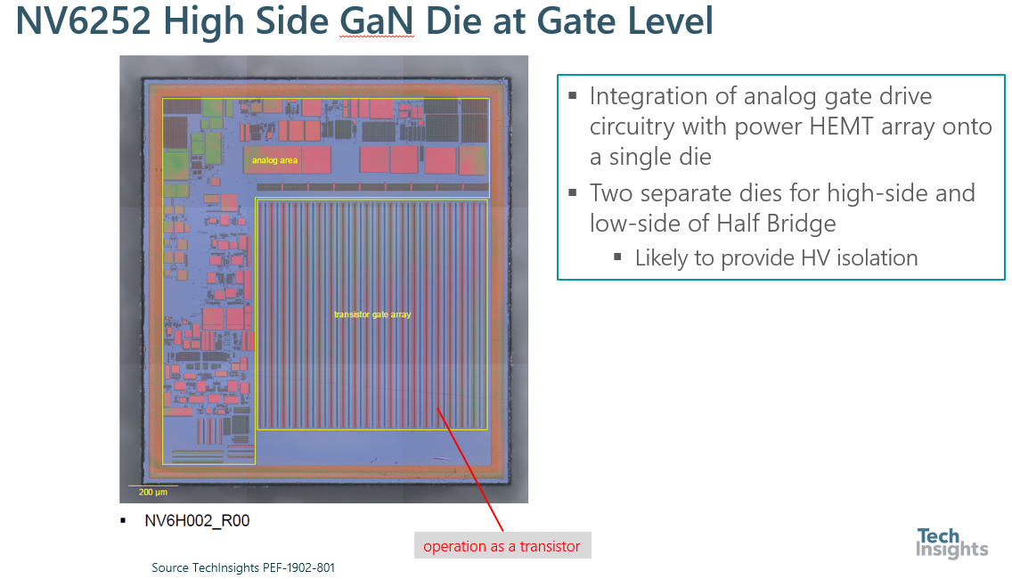
图6 Navitas HV6H002高端模具布局
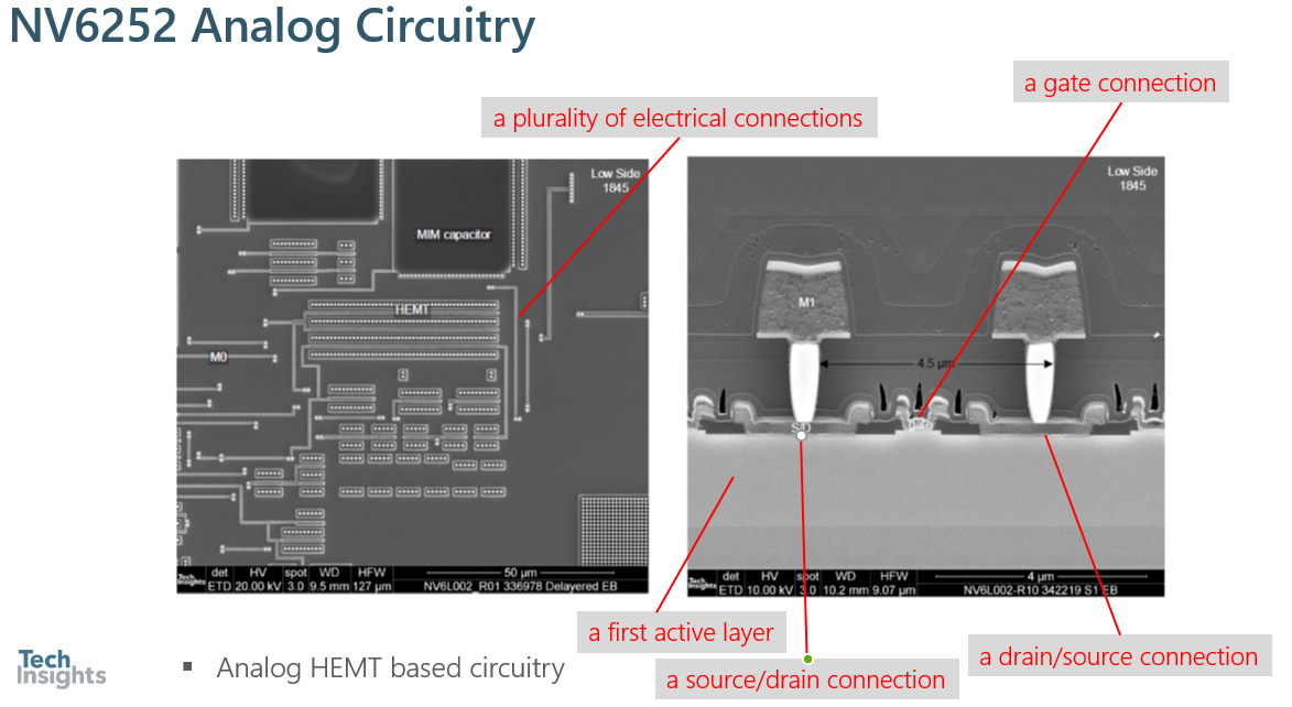
Figure 7 Navitas HV6L002 Low Side Die Analog Circuitry
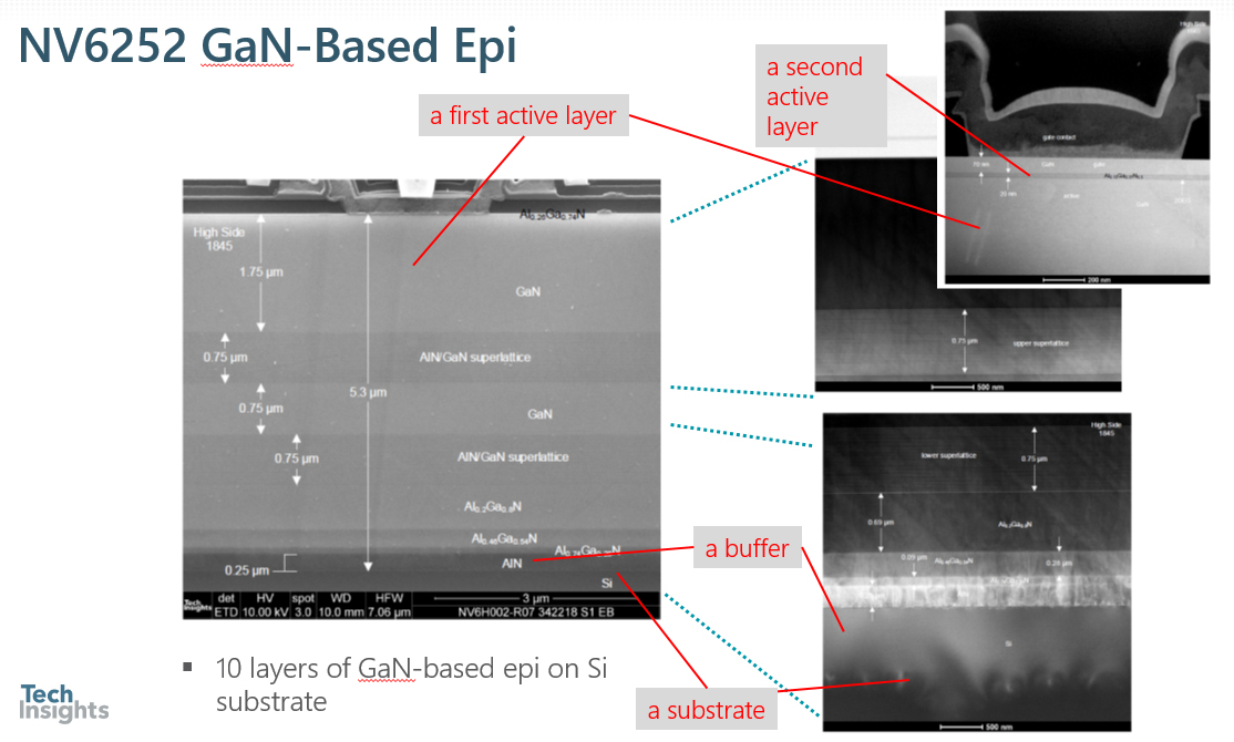
Figure 8 Navitas HV6H002 High Side Die GaN Epitaxial Structure
基于氮化镓的电力电子是半导体技术的一个新兴领域。TechInsights正在越来越多的商业产品中观察Si上的GaN和SiC上的GaN功率晶体管。我们的结果表明,1991年的开创性的987年GaN-HEMT专利现在被广泛使用。然而,978年专利中的概念现在是公开的。自1991年以来,已经有了相当大的创新,包括使用更复杂的GaN基外延,使用Si和SiC衬底,而不是987年专利摘要中描述的蓝宝石(AlO)衬底,常闭操作工程,以及最近的Panasonics混合栅注入(HD-GIT)技术。TechInsights将继续监控这一市场,并将关键创新作为我们业务的一部分进行报告功率半导体Subscription程序。